Published On 20 Oct 2025
A fragile ceasefire is in effect, and the living Israeli captives are back home, but Israel is continuing to restrict humanitarian aid into Gaza. With decimated…

Published On 20 Oct 2025
A fragile ceasefire is in effect, and the living Israeli captives are back home, but Israel is continuing to restrict humanitarian aid into Gaza. With decimated…

Published on: Oct 20, 2025 09:44 am IST

FILE – An arrangement of peanuts is seen Feb. 20, 2015, in New York.
Patrick Sison/APA decade after a landmark study proved that feeding peanut products to young babies could prevent development of life-threatening allergies, new research finds…

If you like playing daily word games like Wordle, then Hurdle is a great game to add to your routine.
There are five rounds to the game. The first round sees you trying to guess the word, with…
The explosive growth of AI is driving a shift from copper to optics in data centers—and transforming photonic integrated circuit production.
[A. Morozov / Getty Images]
The demand for photonics is being pushed to an unprecedented degree by the dramatic scale-up and scale-out of artificial intelligence (AI) infrastructure. As current copper-based networks are stretched to their limit, photonic links are being called upon to overcome bottlenecks in bandwidth, power and latency.
The frenzied interest in fiber networks for data centers that house AI infrastructure—also known as “AI factories”—is paving the way for a new era in photonics manufacturing. In particular, many researchers are focusing on automation in photonics packaging and testing to meet the demand for higher volumes.
“Just looking at the transceivers market, considering AI and the number of users, we anticipate that it will grow much faster and much bigger than before,” said Nikta Jalayer, global portfolio director of Photonics Integrated Circuits at Physik Instrumente, USA. “If it is going to grow, then we need to automate different aspects that are associated with manufacturing photonic integrated circuits.”
The sheer scale of today’s AI models is staggering, with parameter counts now reaching into the billions and even trillions. More parameters—defined as the internal variables whose values are adjusted during training to make predictions—typically translate into a model’s greater power and performance. At its 2019 release, OpenAI’s GPT-2 contained 1.5 billion parameters; GPT-4, introduced a mere four years later, boasts 1.8 trillion parameters.
Exponential growth in both the size and complexity of AI models means an ever-increasing need for more computational power. A study by OpenAI found that the computational power needed to train the largest AI models has doubled in size every 3.4 months since 2012. As a result, AI factories are scaling out at unprecedented levels. While “scaling up” refers to increasing the resources of a single server, such as adding more graphics processing units (GPUs), “scaling out” involves adding more servers to a cluster or distributed system. Hyperscale data centers now house at least 5,000 servers, with possibly miles of connection equipment.
Traditional data centers have long relied on copper-based electrical wires for internal communication networks. But the AI boom, with its requirements of higher bandwidth and data transmission speeds over longer distances, has accelerated the switch to fiber optics.
“Right now, to communicate between different GPUs and racks, the industry is heavily relying on copper and only uses fiber for things like intercontinental transmissions,” said Andon Bano, international sales engineer at ficonTEC, Germany, a company specializing in manufacturing automation solutions. “But fiber is moving more and more inside, because the data requirement to be transmitted even between racks is too high. The copper is saturated.”
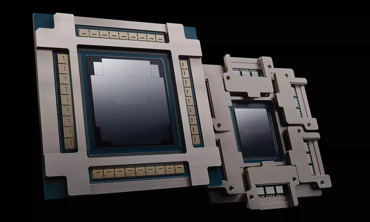 Nvidia has released two networking switches based on silicon photonics technologies. According to the company, the technologies will enable AI companies to connect millions of GPUs. [Courtesy of Nvidia]
Even technology giants like Nvidia, Intel and IBM have moved into the optical connectivity arena. In his keynote speech at GTC 2025 in March, Nvidia CEO and founder Jensen Huang announced the release of Nvidia’s first co-packaged optical networking switches, a compact alternative to the bulky pluggable transceivers used to perform photoelectric conversion.
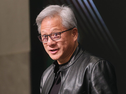 Jensen Huang [總統府 / Wikimedia Commons]
“We use copper as much as we can on scale-up, but on scale-out, where the data centers are now the size of a stadium, that’s where silicon photonics comes in.”
—Jensen Huang, Nvidia CEO and founder
“We should use copper as far as we can—let’s call it a meter or two—and that’s incredibly good connectivity, very high reliability, very good energy efficiency, very low cost,” explained Huang. “We use copper as much as we can on scale-up, but on scale-out, where the data centers are now the size of a stadium, we’re going to need something that’s much more long-distance running. That’s where silicon photonics comes in.”
“Until recently, Nvidia was all about copper—but now they’re realizing copper’s not going to cut it. It gets too hot. There’s too much power consumption and loss,” said Anuradha M. Agarwal, principal research scientist at the Massachusetts Institute of Technology, USA. “So, they had to move to photonics.”
Although progress continues to lag far behind that of microelectronics, the recent investment and pressure to succeed from the AI industry could be enough to advance photonics to a place that can match its electrical counterpart.
Billions of dollars and decades of research have gone into microelectronics manufacturing, resulting in a mature, low-cost, high-yield and robust process. The integration of automation technologies—including robotics, AI and advanced process-control systems—has successfully enhanced efficiency, precision and scalability.
The goal is now to bring some of the lessons learned into the field of photonic integrated circuits (PICs), a technology that integrates photonic devices and optical interconnects onto a chip. The complexity of PICs has increased exponentially since their advent in the mid-1980s. The number of photonic components integrated onto a single chip—now approaching as many as 10,000—has followed a trend similar to Moore’s law in electronics with a delay of 25 to 30 years.
“The integration of photonics and electronics has slowed partly because of the culture—the microelectronics world is very mature, and photonics is still new,” said Peter O’Brien, head of the Photonics Packaging Group at Tyndall National Institute, Ireland. “But the more you familiarize yourself with microelectronics, you can start to make photonics technologies compatible and easier to integrate.”
The first commercial optical transceivers emerged in 2007, with PICs serving as transmitters and receivers at both ends of the optical fiber. As a result of surging demand for optical connectivity in AI factories, sales of lasers and PICs used in optical transceivers are expected to increase from US$2.4 billion in 2023 to US$5.9 billion in 2029, according to market research firm LightCounting.
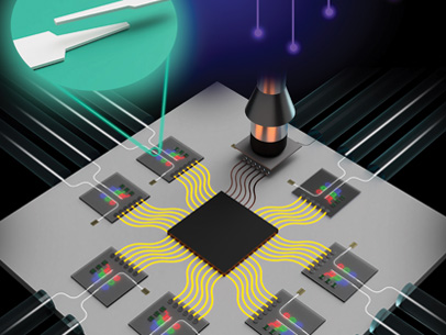
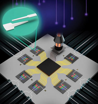 A co-packaged optics system with an electrical chip (black, center) surrounded by eight silicon photonic chips. Chips are bonded using an automated pick-and-place tool, shown placing the final chip into position. The automation is enabled by a novel optical chip-to-chip coupler (green callout). [D. Weninger et al. Adv. Eng. Mat. 27, 2402095 (2025)]
Many experts view co-packaged optics—where the PIC is on the same package substrate as the application-specific integrated circuit (ASIC)—as the future of data centers. Instead of having optical modules connected to switches and routers through electrical interfaces, co-packaged optics significantly reduces the physical distance between the optical and electrical components, increasing bandwidth and enhancing performance.
Yet photonics still lacks a standard technology and production line compatible with legacy microelectronics packaging pipelines that can achieve large-scale integration in line with market demand. For example, since its establishment in 2001, ficonTEC has mainly provided custom ad hoc machinery for assembly or testing of high-end photonic devices, including PICs. The company has delivered more than 1,500 machines to its customers.
“Photonics has been always, let’s say, at a prototyping level. In comparison to semiconductors, photonics has always been in the low- to mid-volume range,” said Bano. “Many of our customers need machines built around their product instead of a standard machine that satisfies different products.”
As the photonics industry moves toward higher volumes and a greater density of integration, the need for standardization, automation and intelligent development of PIC manufacturing solutions increases as well.
Semiconductor manufacturing is incredibly complex, involving hundreds of steps and stretching up to four months from design to mass production. Adding photonic components to the mix complicates things further, with extra steps needed for aligning optics and testing. In particular, the final steps of packaging and testing are crucial to creating a durable and reliable finished product.
Packaging, which can consume more than 80% of the total manufacturing cost, is a notable bottleneck that has impeded the growth of PIC markets. Photonics packaging covers the technology needed to support both optical and electronic interfacing with the PIC and includes fiber coupling, laser-source integration, wire bonding and flip-chip integration for efficient high-speed signaling. It is largely a device-by-device process that is difficult to fully automate and subsequently scale to high volumes.
“If you speak to ficonTEC, the automated systems are very much package by package, and in many cases, it’s automated to a particular company’s requirements,” said O’Brien. “You could imagine an automotive manufacturer, with everybody ordering a slightly different car. It just wouldn’t scale.”
 Peter O’Brien [Courtesy of Tyndall National Institute]
“Automation is much better when we move to wafer level because everything’s on the surface, and it’s much easier to scale.”
—Peter O’Brien, head of Photonics Packaging, Tyndall National Inst., Ireland
Conventional bonding of optical fibers to the PIC device uses an active alignment procedure where the coupled optical power is continuously measured and maximized. The fiber is then fixed in position, or bonded, with UV-curable epoxy. Because it is performed at the component or package level, it suffers from throughput limitations, with cycle times on the order of minutes to tens of minutes per package.
O’Brien’s research focuses on moving the industry to wafer-scale packaging, akin to microelectronics manufacturing, to achieve significantly higher throughputs—cycle times of seconds per device—by using parallel alignment. By shifting optical interfaces to the PIC surface instead of the PIC edge or facet (as with standard fiber coupling), manufacturers can enable wafer-scale packaging and automation of the alignment procedure using machine vision. Surface connections will also allow for more optical channels via 2D arrays instead of being restricted to only linear arrays on the edge.
“For machine vision systems, aligning to the edge of the waveguides on a chip is very challenging, especially with the alignment tolerances that are needed,” he said. “Automation is much better when we move to wafer level because everything’s on the surface, and it’s much easier to scale.”
Recently, O’Brien’s lab demonstrated the first 90° turning mirror micro-lens scheme for coupling of light from a transceiver PIC edge coupler to the optical fiber. The team employed a specially manufactured silicon micro-lens equipped with an etched turning prism to take advantage of the superior performance of edge couplers and turn them into surface features for easy integration.
The vertical coupling lens has three primary working surfaces: a first curved surface that takes the expanding beam and collimates it to interface with the connector, a second smooth surface that minimizes scattering of light, and a third surface responsible for the total internal reflection of light. The approach has an expanded beam connection, relaxing the alignment tolerances of the connector, which itself is composed of a fiber array with a micro-lens attached to the facet.
Using this approach, O’Brien and colleagues demonstrated sub-2 dB coupling loss at 1310 nm from a transceiver chip. The achieved relaxation of tolerances to around 28 μm is roughly 35 times the typical alignment precision necessary for butt-coupling an optical fiber to the PIC in standard packaging. With further development toward a low-profile surface-mounted coupling scheme, assembly of such a device can be automated by taking advantage of precision alignment of elements with machine vision.
The research is being conducted in close partnership with industry as part of a pilot line for photonics packaging. With O’Brien acting as director, the PIXAPP Photonics Packaging Pilot Line will establish what it believes is the world’s first open-access PIC assembly and packaging service to bridge the “valley of death” from lab to market.
“You have research, and you have commercialization, but there’s this gap in the middle. Does industry reach back, or do the researchers push forward?” O’Brien said. “It’s what they call the valley of death, and the European Commission has developed a pilot line to address that. It’s an accelerator for research, but it’s also a way to move things into industry.”
For co-packaged optics, the scaling of bandwidth capacity, energy efficiency and cost per package is associated with the number of transceivers per package. Because photonic elements such as micro-ring modulators and photodetectors take up a much larger area than their electronic counterparts, vertical stacking of PICs will become a necessity. However, the creation of another optical-optical interface poses loss and alignment challenges.
Agarwal’s lab has come up with a novel solution: a vertical optical interconnect design with low insertion loss, high translational and rotational alignment tolerance, and complementary metal-oxide semiconductor (CMOS) process flow compatibility. The design leverages evanescent coupling through an optical interposer, much like an electrical interposer is used to interface between adjacent electronic devices.
In the past, evanescent coupling had been able to couple one waveguide to another on the same chip thanks to precision lithography. “Now think about doing the same thing with two separate chips,” she said. “You can create waveguides using lithography, but when you’re putting two chips together—let’s say you’re flip-chipping one on top of another—now all bets are off in terms of the Z distance.”
For co-packaging applications, Agarwal and colleagues designed a robust, vertical evanescent coupler for coupling between two separate chips or from interposer to chip (as opposed to coupling between two layers of the same chip). It consists of two overlapping, inverse double tapers with one waveguide made of silicon and the other made of silicon nitride (SiN), which leads to a reduction in propagation loss on the interposer due to the lower refractive index of SiN.
“The alignment tolerance is helped when we use our double-taper design, because now we don’t have just a single point at which light jumps from one waveguide to another, even when the effective indices match,” said Agarwal. “Instead, it has a longer length over which such a transition can happen.”
In a 2024 study, the team experimentally demonstrated the vertical chip-to-chip evanescent coupler with 0.39-dB coupling loss at 1550 nm and an average loss of 0.72 dB across the C-, S-, and L-bands (1480 to 1640 nm). The coupler achieved an average 1-dB lateral alignment tolerance of 1.38 μm for the 1480 to 1640 nm wavelength range, enabling passive assembly using automated pick-and-place technology.
“You can also envision doing the same for an evanescent coupler from chip to fiber, but how can we find a way to get the light up to the top and then eventually couple it to a fiber?” Agarwal said. “Maybe couple from one chip to another with the evanescent coupler, and from that chip go to a fiber using a microreflector at the end. These are the ideas that we’ve been tossing around, and this is our next research direction.”
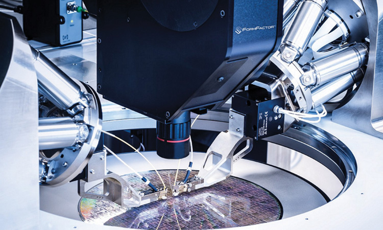 FormFactor CM300 silicon photonics wafer prober with PI F-712.HA2 dual hexapod and piezo scanner alignment system. [FormFactor]
Photonic device testing is another area that could benefit from improvements in standardization and automation. Because testing is needed across the full value chain, it can consume as much as 29% of total PIC manufacturing cost. Testing spans from front-end processes in a photonic foundry through back-end testing of bars, dies, subassemblies and modules, and, ultimately, system-level evaluation.
In particular, the recent rise of co-packaged optics sets new limitations on testing, since the technology integrates PICs directly alongside the ASIC or on the package substrate. The functionality, performance and reliability of the PIC components must be verified before being permanently co-packaged with electronic components, since component replacement is no longer possible after assembly.
Testing is a critical, technically demanding step that requires high-precision optical alignment and measurement. Companies like ficonTEC, FormFactor, EXFO and Keysight are developing next-generation automation solutions to speed up the process.
For example, FormFactor has partnered with precision motion specialist Physik Instrumente to develop a fully automated and reliable probing system to test silicon photonics devices in wafer and die form. The CM300xi-SiPh probe station is equipped with the Autonomous Silicon Photonics Measurement Assistant, which precisely calibrates the optical positioning hardware to the probe station and verifies the performance of the integrated system.
The system employs two of Physik Instrumente’s hexapods—parallel-kinematic motion platforms that position and align loads in six degrees of freedom—to perform precise alignment of optical probes with nanoscale accuracy. “Our systems are doing what the industry believes is one of the most difficult and critical aspects of these types of tests, which is the alignment aspect,” said Jalayer. “It might seem very simple, but the levels of accuracy we’re dealing with—nanometers versus microns in electrical testing—as well as the fact that you cannot really get too close, is very different than other industries.”
ficonTEC is advancing higher levels of automation and highly parallel, mixed-signal electro-optical testing concepts—both on- and off-wafer. The company’s testing platforms focus on automated electrical, optical or mixed-signal electro-optical characterization of chips and dies, optoelectronic assemblies and integrated devices, supporting PIC design validation and device verification.
In March, ficonTEC introduced a high-volume, double-sided wafer probe test cell for silicon photonics, designed to be compatible with existing semiconductor automated test equipment (ATE) and targeted for AI factory applications. The technology directly docks with the ATE at a core software and hardware level, enabling electrical testing on the top side and six-axis active optical alignment probing below.
“What has been happening so far in these foundries is that they do the electrical testing first, and then they take the wafer out and do the photonics testing,” said Bano. “We and other companies had been offering photonic electro-optic testing for photonic chips, but they were not in the standards that the foundries were looking for. They were not compatible with the ATEs, until now.”
ficonTEC has partnered with Teradyne, a leading ATE provider, to offer high-throughput testing of silicon photonics at the wafer level to foundries facing the surging demand for co-packaged optics. The integrated test cell combines Teradyne’s ATE and programming environment with ficonTEC’s advanced optical-alignment, probing and wafer-handling technologies. Now, foundries can discard bad chips before wafers are diced and packaged into co-packaged optical devices or pluggable transceivers.
 Anuradha M. Agarwal [Courtesy of MIT]
“The importance of co-packaged optics today is almost like way back when the transistor was invented at Bell Labs—everything changed in the field of electronics.”
—Anuradha M. Agarwal, MIT, USA
Right now, PIC manufacturing is still in its infancy, especially compared with microelectronics. But that is quickly changing under mounting pressure from AI factories and other data centers that need more advanced networking solutions.
“AI factories are a new class of data centers with extreme scale, and networking infrastructure must be reinvented to keep pace,” said Nvidia’s Huang in a March press release. “By integrating silicon photonics directly into switches, Nvidia is shattering the old limitations of hyperscale and enterprise networks and opening the gate to million-GPU AI factories.”
Nvidia’s co-packaged optics–based networking switches boast needing 4× fewer lasers to deliver 3.5× more power efficiency, 63× greater signal integrity, 10× better network resiliency at scale, and 1.3× faster deployment compared with traditional methods. The demand for such technology will only continue to grow, and as a result, photonics manufacturers must find ways to adapt to higher volumes and a faster pace of innovation.
“The importance of co-packaged optics today is almost like way back when the transistor was invented at Bell Labs—everything changed in the field of electronics,” said Agarwal. “My sense is, once we enter the co-packaged era, we’re never going to look back. It’s going to be a completely different world.”
Automation is key to addressing many of these challenges. It can rapidly scale volume while lowering the dependence on labor, which will ultimately reduce costs, optimize production and sustain a competitive edge. While some innovations like automated active alignment have already had a notable impact on the industry, introducing AI into manufacturing processes is the logical next step.
Physik Instrumente is working on several new alignment algorithms that incorporate AI for industrial photonics applications, spanning wafer probing through final packaging. In 2024, Physik Instrumente introduced its fully autonomous PILightning algorithm for photonic alignment, designed to eliminate time-consuming search routines or manual intervention. PILightning can achieve first-light detection through a search method with integrated AI-based real-time executive function.
Another area of research is passive alignment, such as photonic wire bonding, which uses computer vision and simple alignment markers to locate the coupling sites. “If you’ve got very precise, lithographically defined alignment marks, then you can basically pick up a part and place it with very, very high accuracy on the surface. The machine vision systems are well able to do that,” said O’Brien. “But they can’t do that on the edge, so once you move to the surface, you can start to do what we call passive alignment more and more.”
Through such innovations, photonics manufacturers can leverage automation to stay ahead of the curve and ensure the continued advancement of what big tech regards as critical infrastructure. “Even five years ago, people were thinking about photonics as Disney’s version of a stepchild: People knew of its existence, but no one really cared so much,” said Agarwal. “But now that you see Nvidia, Intel, Apple—everybody’s jumped onto this bandwagon, including foundries like TSMC, Samsung and so on. They’re realizing that, ‘Well, photonics is actually our very dear child, and we can’t move forward without it.’”
Meeri Kim is a freelance science journalist based in Los Angeles, CA, USA.
For references and resources, visit: optica-opn.org/link/photonics-ai-factories.
A synthetic chemical…
The news: The Trade Desk’s connected TV (CTV) operating system, Ventura, is entering a crowded market dominated by giant tech players like Amazon—but TTD views the operating system as a yearslong bet on increasing transparency in the CTV…

William Shakespeare coined the phrase “brave new world,” which is often used to describe the astonishing possibilities and potential problems of technological advancements.
But he probably never envisioned teachers would make his plays come…