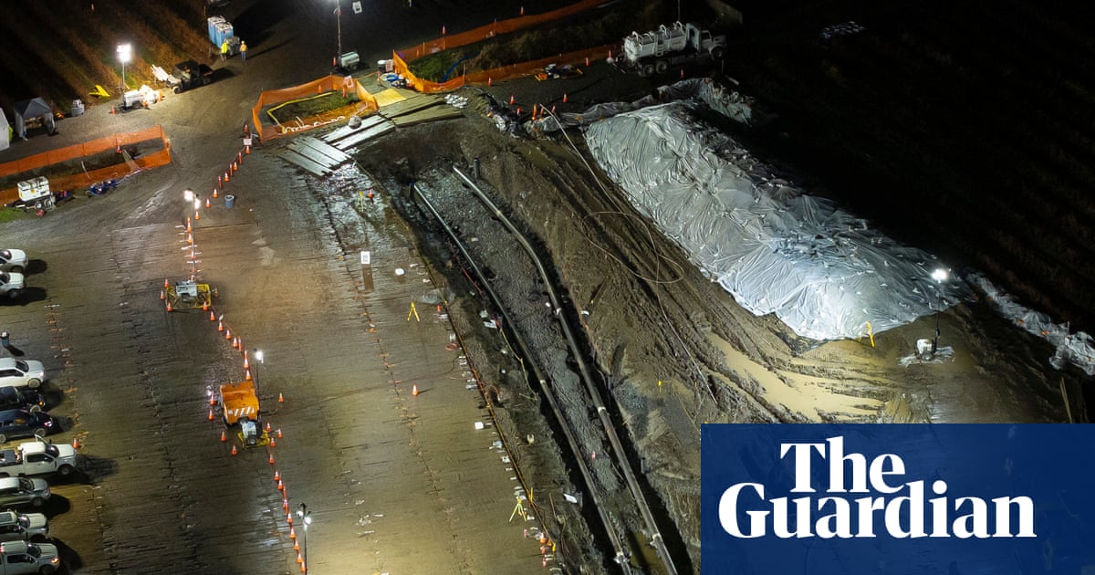
Investigators have identified the source of a leak in the Olympic pipeline two weeks after fuel was first spotted in a ditch near an Everett, Washington, blueberry farm.
Oil and gas company BP, the operator of the pipeline, shared in a statement that it had determined the leak occurred in a 20in pipeline and not a neighboring 16in pipeline, allowing that pipeline to be restarted.
“Repair plans for the 20-inch segment are being developed and a timeline for repair and restart will be shared when available,” BP said.
The news follows announcements by the Washington and Oregon governors, Bob Ferguson and Tina Kotek, respectively, declaring states of emergency due to the disruptions in fuel supplies. The Olympic pipeline carries gasoline, diesel, jet fuel and other petroleum products to both states, including 90% of Oregon’s transportation fuel and much of the Seattle-Tacoma international airport’s jet fuel.
The leak was first reported on 11 November between the Washington towns of Everett and Snohomish. The state department of ecology determined the leak consisted of a combination of gasoline, jet fuel and diesel. BP shut off two pipelines that ran side by side in the Olympic pipeline system to determine the source of the leak, either a 16in or a 20in pipeline.
On 16 November, the company restarted the 16in pipeline, but shut if off again after observing “an increase in product observed in a collection point”, it said in a statement.
Later that week, on 19 November, Ferguson issued a state of emergency in Washington, waiving state regulations to allow commercial vehicle operators to drive longer hours to transport jet fuel to Seattle-Tacoma airport.
Kotek followed suit in Oregon on Monday, declaring a similar state of emergency and waiver of commercial driving regulations.
In statements to Reuters on Monday, major airlines operating through Seattle-Tacoma and the airport itself said they had developed contingencies to prevent disruptions to holiday travel.
“We do not expect disruption to our operations at Seattle-Tacoma international airport through the Thanksgiving travel week,” Alaska Airlines said, adding that it had brought extra fuel into Seattle on inbound flights and additional trucking shipments, and added fuel stops to certain flights.
Delta Air Lines similarly said it had transported additional fuel to the airport and added refueling stops to some long-haul flights.
On Monday, BP reported that it had excavated “over 200 feet of pipeline” and expected to “continue overnight operations tonight”. By Tuesday morning, the company had found the source of the leak.
In updated statements to Reuters on Tuesday, Delta said it “is operating our full Seattle hub schedule and has discontinued fuel stops on select long-haul flights”. Alaska added that it had “discontinued all planned fuel stops but will continue to tanker and truck in additional fuel on a reduced basis as the pipeline increases to normal capacity”.
Repairs to the 20in pipeline come as Washington state’s ecology department has fined BP $3.8m for a 2023 gasoline spill from the Olympic pipeline. The Olympic pipeline has leaked at least 13 times since 1999, when a leak near Bellingham caused an explosion that killed a teenager and two younger children. According to the Pipeline Safety Trust, a Washington state-based non-profit, the pipeline has leaked three times in 2025.
“These incidents have caused over $100m in property damage,” Kenneth Clarkson, spokesperson for the Pipeline Safety Trust, said in a statement to the Associated Press. “Olympic Pipeline must explain what has changed and what they’re doing to stop it.”