Closing out the machine learning sessions at Hot Chips 2025 is Google, who is at the show to talk about their latest tensor processing unit (TPU), codenamed Ironwood. Revealed by the company a few months ago, Ironwood is the first Google TPU that is explicitly designed for large-scale AI inference (rather than AI training). Paired with a strong model, and Ironwood is intended to excel at LLMs, mixture-of-expert, and reasoning models.
With up to 9,216 chips in a node, Ironwood can scale up to 42.5 Exaflops in performance. Though with 10MW of power consumption, that performance doesn’t come cheap. All told, Ironwood is said to offer 2x the perf-per-watt of Google’s previous generation TPU, Trillium. But, like all of Google’s TPUs, this is solely for Google’s use as part of their Google Cloud services, so Ironwood is not available to look at outside of Google. This makes TPU presentations at Hot Chips potentially very insightful, offering details that could not otherwise be easily gleamed.
Ironwood TPU comes with several innovations. And that will be the focus of today’s talk (rather than reciting pedestrian improvements).
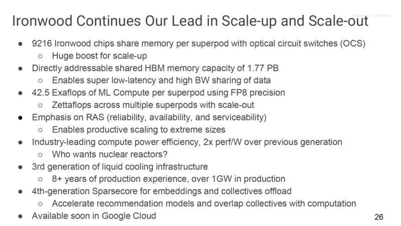
The big one is how big the SuperPods can go. Now up to 9,216 chips, thanks to the use of optical circuit switches (OCS) to share memory throughout the pod. There’s 1.77 PB of directly addressable HBM altogether.
This generation also brings a focus on RAS features in order to have reliable systems.
Power efficiency also gets a boost, of course. Google is claiming a 2x perf-per-watt improvement – though it’s unclear if this is at iso-datatype.
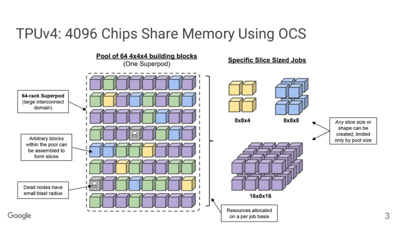
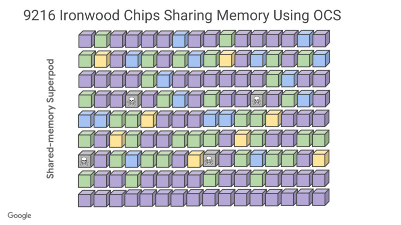
Comparing Ironwood to TPUv4 using optical circuit switching. Ironwood doubles the number of chips within a pod. OCS allows for pods to be configured into different sizes of rectangular prisms. And OCS can drop dead nodes, reconfiguring a slice to use other racks by restoring from a checkpoint. (This happens frequently, we’re told – checkpointing, that is, not nodes dying)
9216 is a bit larger than a power-of-two in order to have extra racks for RAS reasons. (8192 leaves no spares)
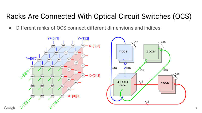
And here’s another look at OCS, and how it’s organized as a 3 dimensional logical arrangement of nodes.
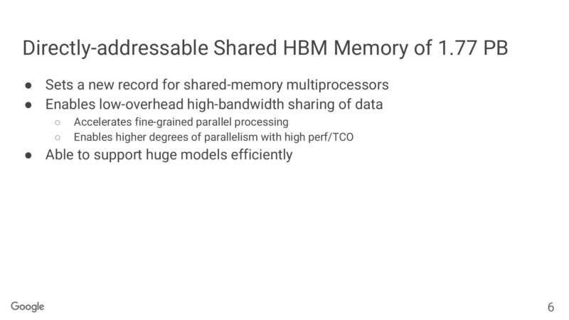
With 1.77PB of HBM, Google has set a new record for how much shared memory is available.
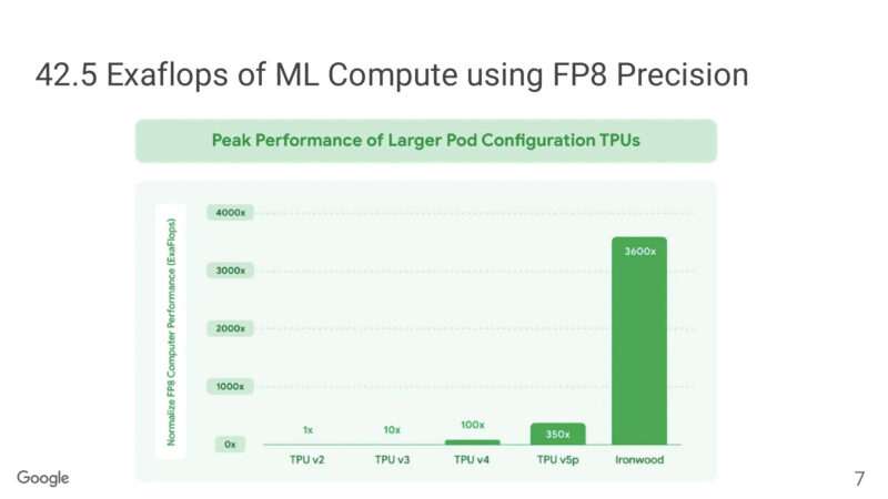
Meanwhile a look at compute performance with FP8. Ironwood is a massive step up in this regard.
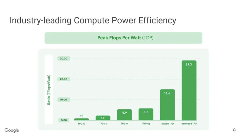
There’s a close to 6x improvement in perf-per-watt versus TPUv4
And again, noting that they have focused on RAS with this generation. Cloud TPU instances need to be able to go a long (and ever longer) time without errors.
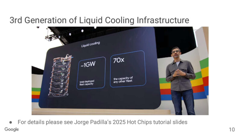
Ironwood also comes with Google’s third generation of liquid cooling. Google uses multiple loops to keep the water going into the cold plate very clean, least it plugs up the plate.
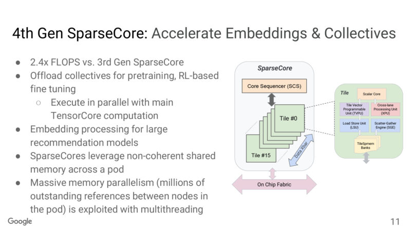
Ironwood also offers the latest generation of Google’s SpareCore functionality.
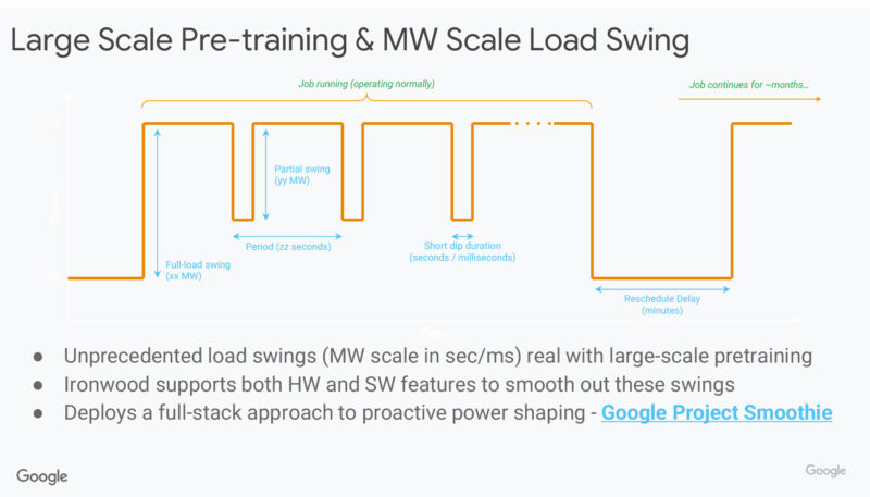
There’s also been a focus on not just power efficiency, but power stability as well. Google has hardware and software features to smooth out power consumption swings in order to make things earlier on electric utilities.
And a quick video roll confirms that hyperscale deployments are underway.
Now diving a bit deeper into the Ironwood architecture.
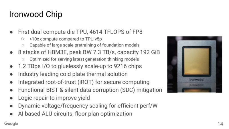
Google updated the SoC architecture so that it could scale beyond a single die, so they aren’t reticle limited. Consequently, Ironwood is their first multiple compute chiplet die, with two Ironwood compute dies on each chip.
A renewed focus on the memory subsystem in order to better feed LLMs means that Google has gone with 8 stacks of HBM3e memory, allowing for 192GB of memory with 7.3TB/second of bandwidth.
With all that said, Ironwood could not be just about speeds and feeds. Which is why more features for reliability and security are integrated, such as an integrated root of trust, built-in self testing, and functions to catch silent data corruption. There are even functions to check the arithmetic while a workload is being run.
“We put a lot of features in the chip to essentially make this the most power-efficient chip”
And AI has come full circle for these AI chips, as AI was used in designing the ALU circuits and optimizing the floor plan. Google collaborated with their AlphaChip team in this endeavor.
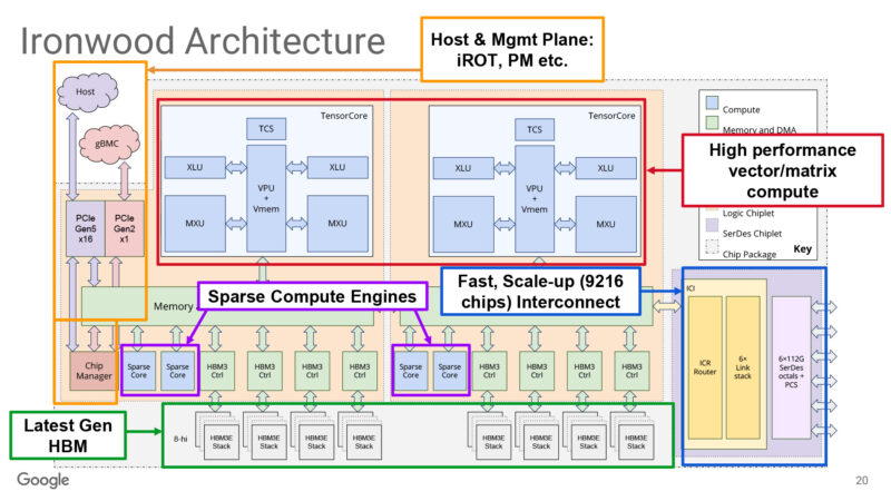
And a logical block diagram of Ironwood, outlining the various major upgrades and enhancements to the TPU architecture. HBM3e is a big deal here, as is the interconnect hardware that allows it to scale up to 9216 chips for one SuperPod. Meanwhile scale-out can go to tens of SuperPods.
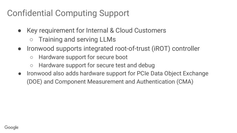
Outlining the various additions to support confidential compute on Ironwood. An integrated root of trust, as well as secure boot and secure test/debug.
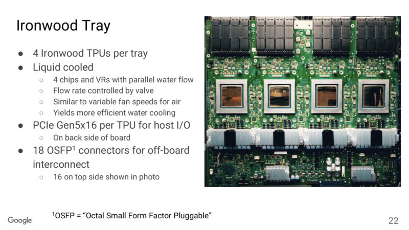
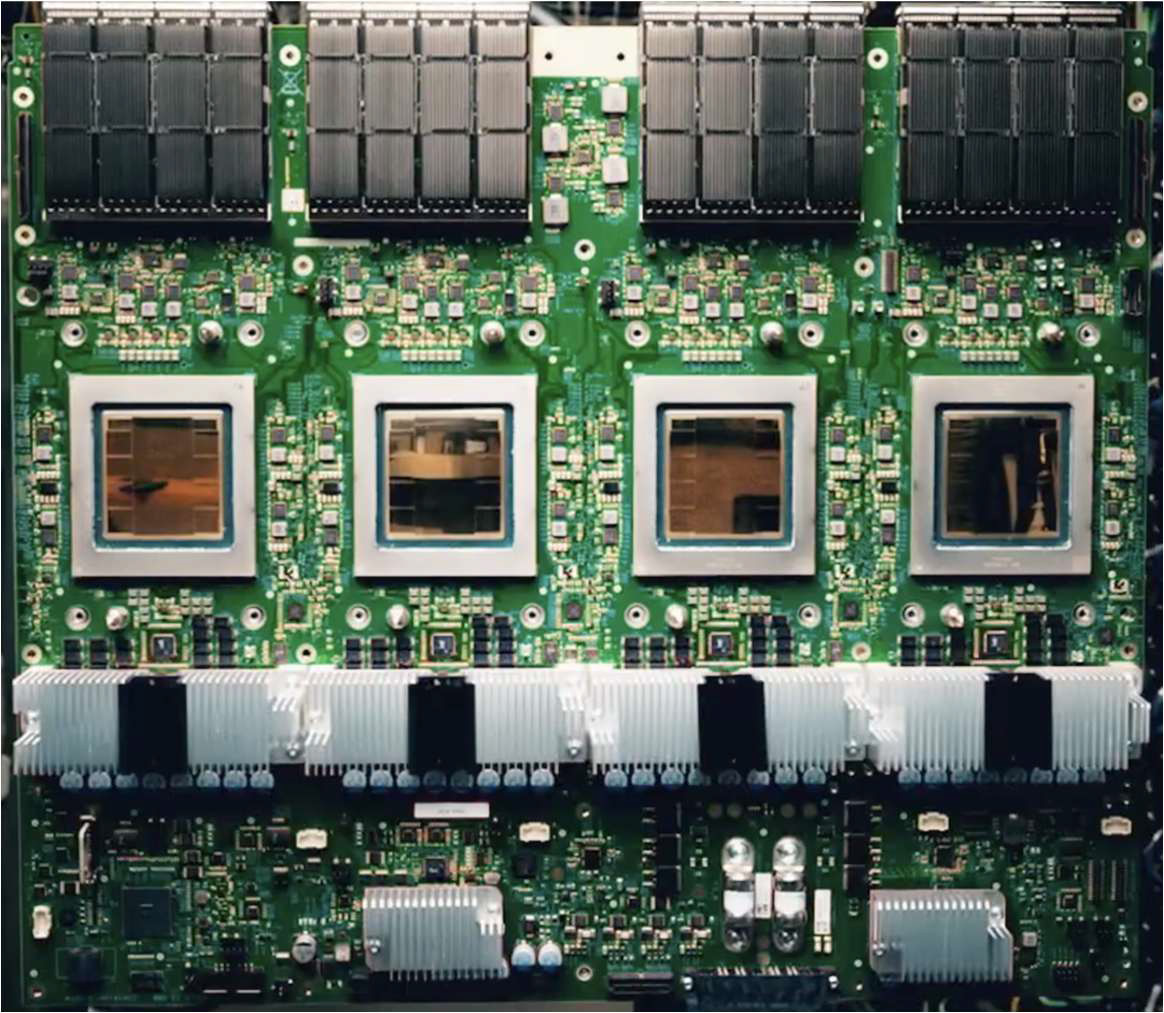
Going above a single chip, here’s a look at an Ironwood tray. Each tray contains 4 Ironwood TPUs. The tray is liquid cooled.
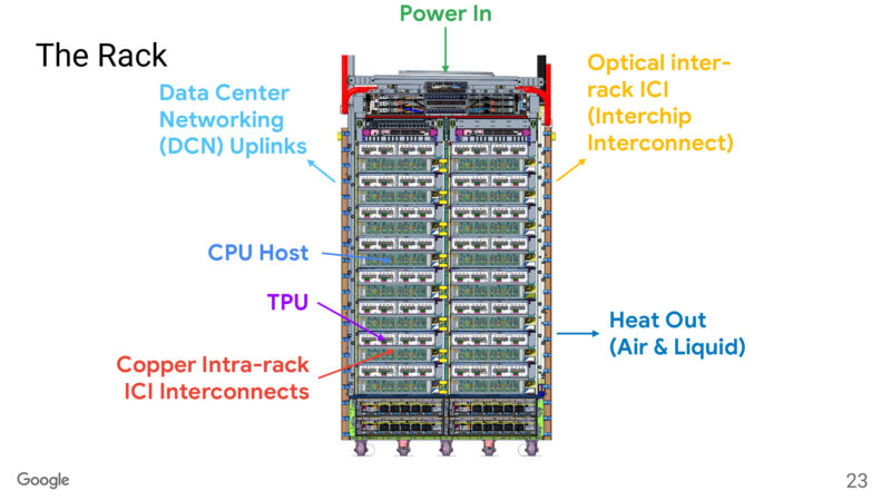
Going up another level, 16 TPU trays go into a rack, for 64 TPUs per rack. This is joined with another 16 CPU host racks. All interconnects within a rack is copper; OCS provides connectivity to other racks.
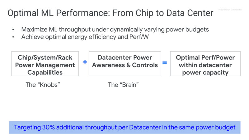
And again, power efficiency is critical here. Power is the constraining factor to overall performance. Delivering on that efficiency doesn’t just mean making good hardware, but combining that with data center-level power awareness and controls to help orchestrate the hardware and ensure the entire data center is running as efficiently as possible.
And that is the Ironwood overview. Google is delivering a big improvement in performance and power efficiency, but this is being coupled with a heavy focus on RAS features in order to deliver the kind of reliability needed for a massive SuperPod to be viable.