As Leica celebrates a century of developing some of the world’s finest photographic equipment, it has made a controversial move by offering an electronic viewfinder (E.V.F.) in place of the old-school mechanical rangefinder in its revered…
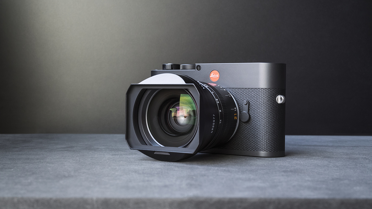
As Leica celebrates a century of developing some of the world’s finest photographic equipment, it has made a controversial move by offering an electronic viewfinder (E.V.F.) in place of the old-school mechanical rangefinder in its revered…