Imagine trying to paint with a brush that randomly changes size and color, frustrating, right? That’s been the challenge with using amorphous zeolitic imidazolate framework (aZIF) films in high-tech applications like electron beam and extreme ultraviolet lithography. These films also show promise for separating molecules in thin membranes, but until recently, making them was more guesswork than precision.
The process relied on trial-and-error, making it challenging to control the thickness of the films, their evenness of spread, and their adaptability to different surfaces.
Enter the team at Johns Hopkins, who cracked the code. They discovered new materials and a more innovative way to deposit aZIF films with precise control over thickness, bringing order to the chaos and unlocking new possibilities for advanced manufacturing and molecular separation.
Their breakthrough could advance the ever-escalating quest to make smaller, faster, and affordable microchips used across modern electronics.
Their discovery could be a game-changer in the race to build microchips that are smaller, faster, and more affordable, the lifeblood of modern electronics. The scientists have figured out how to etch circuits so tiny they’re invisible to the naked eye, using a method that’s both razor-sharp in precision and friendly to large-scale manufacturing.
Scientists Developed Photonic Microchips that Mimics the Human Brain
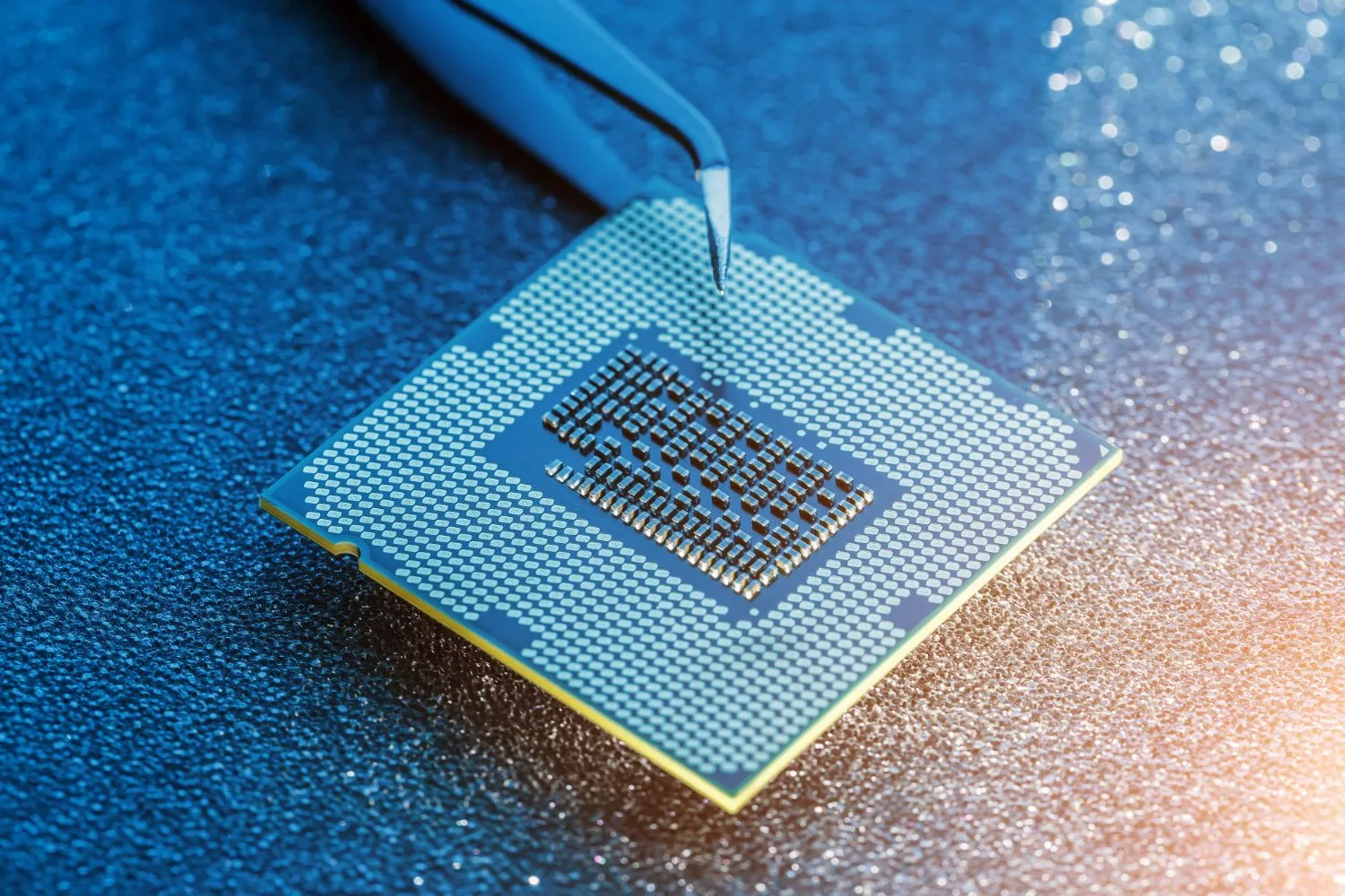
Here’s how it works: microchips start as flat slices of silicon. These wafers are coated with a special material called a “resist,” which reacts to radiation. When a focused beam hits the resist, it triggers a chemical reaction that carves intricate patterns into the surface, laying down the circuitry that powers everything from smartphones to satellites.
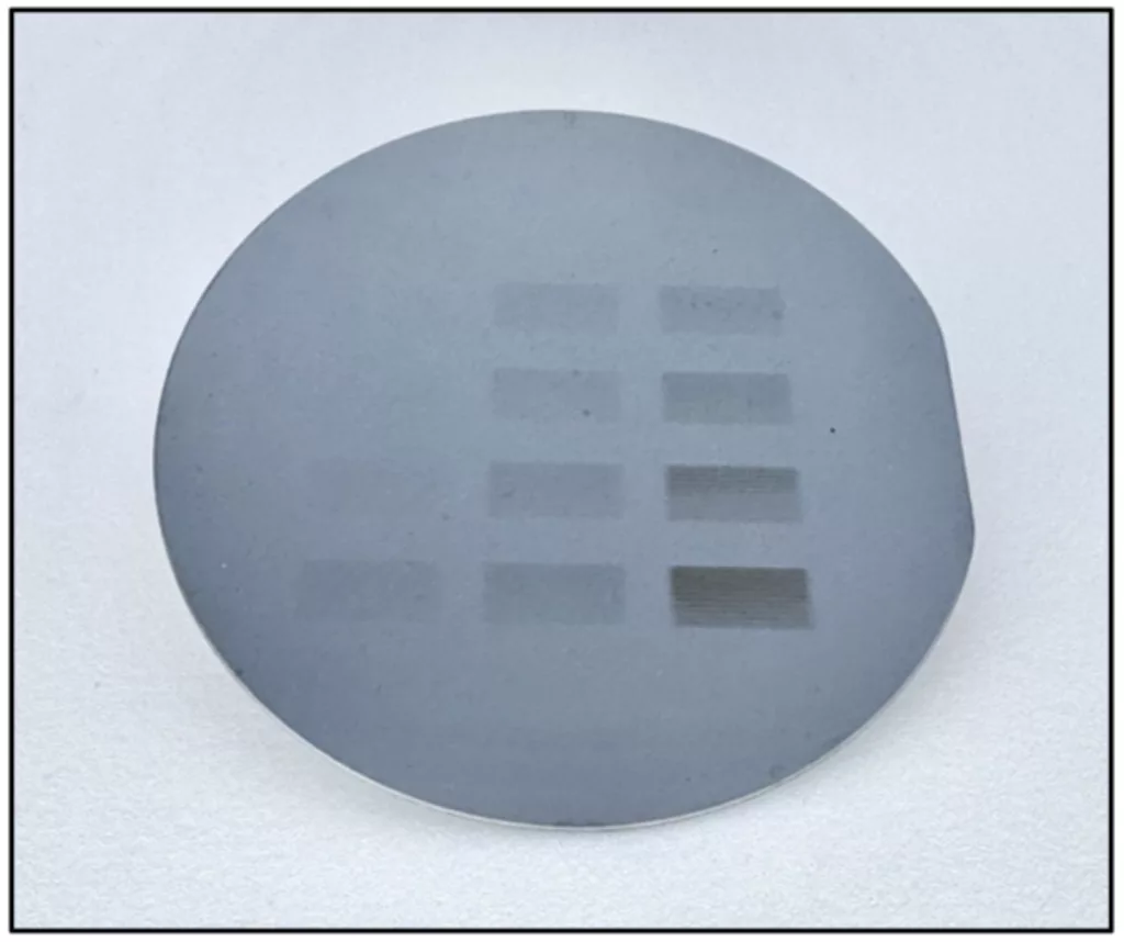
Image credit: Xinpei Zhou
Shrinking microchip features down to the tiniest possible scale requires radiation beams far more intense than what traditional materials can handle. The problem? Standard resists, the coatings used to etch circuit patterns, don’t respond well to this high-powered light.
But researchers from Tsapatsis’s lab and the Fairbrother Research Group at Johns Hopkins found a clever workaround. They developed a new type of resist made from metal-organic compounds that can stand up to “beyond extreme ultraviolet radiation,” or B-EUV. This cutting-edge radiation can carve out features smaller than 10 nanometers, well below today’s standard.
Here’s how it works: metals like zinc soak up the B-EUV light and release electrons, which then trigger chemical reactions in an organic material called imidazole.
This study marks one of the first times that researchers successfully deposited imidazole-based metal-organic resists from solution directly onto silicon wafers, controlling the film thickness down to the nanometer. This breakthrough brings precision and scalability to a process that was previously unpredictable and hard to replicate.
3D inductor technology increases microchip capability
To crack the chemistry behind this feat, the team drew on a global collaboration, blending experimental insights and modeling expertise from Johns Hopkins University, East China University of Science and Technology, École Polytechnique Fédérale de Lausanne in Switzerland, Soochow University in Taiwan, Brookhaven National Laboratory in New York, and Lawrence Berkeley National Laboratory in California.
The result is a new technique called chemical liquid deposition, or CLD, a method that’s not only finely tunable but also fast. It allows researchers to mix and match different metals and imidazoles with ease, opening the door to rapid innovation in chip design and fabrication.
“By playing with the two components (metal and imidazole), you can change the efficiency of absorbing the light and the chemistry of the following reactions. And that opens us up to creating new metal-organic pairings,” Tsapatsis said. “The exciting thing is there are at least 10 different metals that can be used for this chemistry, and hundreds of organics.”
Researchers are now diving into a mix-and-match phase, testing different combinations of metals and imidazoles to find the perfect pairings for beyond extreme ultraviolet (B-EUV) radiation, a powerful tool expected to shape chip manufacturing within the next decade.
As Tsapatsis explains, “Because different wavelengths have different interactions with different elements, a metal that is a loser in one wavelength can be a winner with the other. Zinc is not very good for extreme ultraviolet radiation, but it’s one of the best for the B-EUV.”
Journal Reference:
- Miao, Y., Zheng, S., Waltz, K.E. et al. Spin-on deposition of amorphous zeolitic imidazolate framework films for lithography applications. Nat Chem Eng (2025). DOI: 10.1038/s44286-025-00273-z