Olympic curling champion Eve Muirhead is determined to make her personal journey count as she steps into Team GB’s chef de mission role for the Olympic Winter Games Milano Cortina 2026 in 100 days’ time.
In a recently published autobiography,…
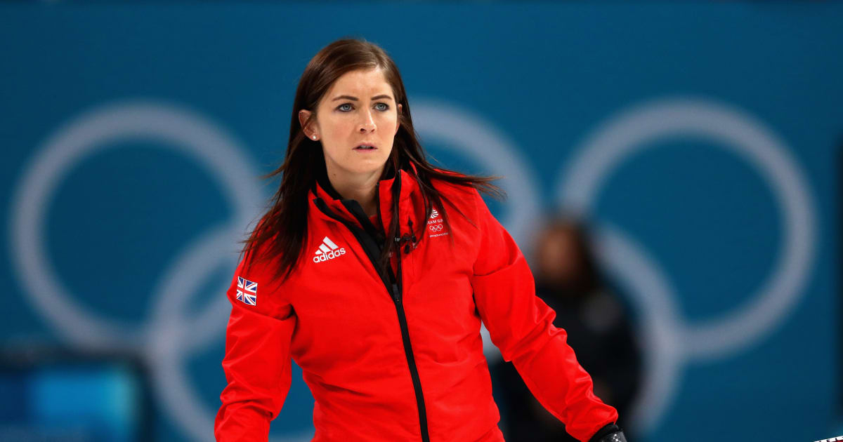
Olympic curling champion Eve Muirhead is determined to make her personal journey count as she steps into Team GB’s chef de mission role for the Olympic Winter Games Milano Cortina 2026 in 100 days’ time.
In a recently published autobiography,…