Paleontologists have identified a new Early Miocene species of the rhinocerotid genus Epiaceratherium from the fossilized remains found in the Canadian High Arctic.
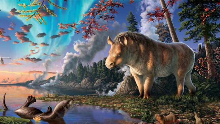
Life restoration of Epiaceratherium itjilik, at its forested lake habitat,…
Paleontologists have identified a new Early Miocene species of the rhinocerotid genus Epiaceratherium from the fossilized remains found in the Canadian High Arctic.
Life restoration of Epiaceratherium itjilik, at its forested lake habitat,…