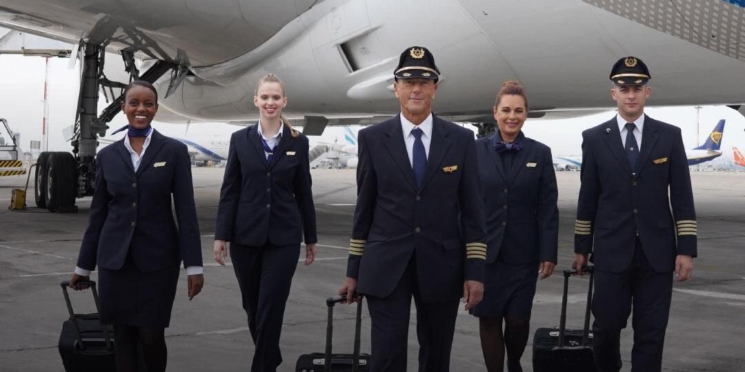
Researchers at Harvard University have developed a new method for conducting complex quantum operations using a single, flat optical device.
This device, known as a metasurface, can perform the functions of multiple conventional optical components, addressing a persistent technical hurdle in the field of photon-based quantum information processing.
“In the race toward practical quantum computers and networks, photons — fundamental particles of light — hold intriguing possibilities as fast carriers of information at room temperature,” said the researchers in a press release.
However, controlling these photons typically requires a large number of discrete components like lenses, mirrors, and beam splitters. Entangling photons, a quantum process necessary for parallel computation, involves creating intricate networks of these parts.
“Such systems are notoriously difficult to scale up due to the large numbers and imperfections of parts required to do any meaningful computation or networking,” explained the press release.
The research team at the Harvard John A. Paulson School of Engineering and Applied Sciences (SEAS), led by Professor Federico Capasso, has engineered a single metasurface to replace such complex setups.
A metasurface is an ultra-thin planar device patterned with nanoscale structures that are smaller than the wavelength of light. These structures work together to precisely manipulate the properties of light, such as its phase and polarization.
“We’re introducing a major technological advantage when it comes to solving the scalability problem,” said Kerolos M.A. Yousef, a graduate student and the paper’s first author.
“Now we can miniaturize an entire optical setup into a single metasurface that is very stable and robust.”
Developing new design process
A key part of the team’s work was developing a new design process to handle the mathematical complexity of multi-photon quantum states. They applied graph theory, a field of mathematics that represents connections within a network.
In this context, the points and lines of a graph were used to map the required interference pathways between photons.
This abstract graph was then translated into the physical layout of the nanoscale patterns on the metasurface.
“With the graph approach, in a way, metasurface design and the optical quantum state become two sides of the same coin,” noted research scientist Neal Sinclair. This method provides a systematic way to construct the device needed to generate a specific, complex quantum state.
Design minimizes optical loss
The resulting metasurface offers several practical benefits. Its monolithic design is inherently more stable and less susceptible to environmental perturbations than a setup built from many individual parts.
It is fabricated using techniques common in the semiconductor industry, suggesting a path toward cost-effective and reproducible production. Furthermore, the design minimizes optical loss, an important factor for maintaining the integrity of quantum information.
The application of this technology could extend beyond quantum computing.
“The work embodies metasurface-based quantum optics which, beyond carving a path toward room-temperature quantum computers and networks, could also benefit quantum sensing or offer ‘lab-on-a-chip’ capabilities for fundamental science,” concluded the press release.