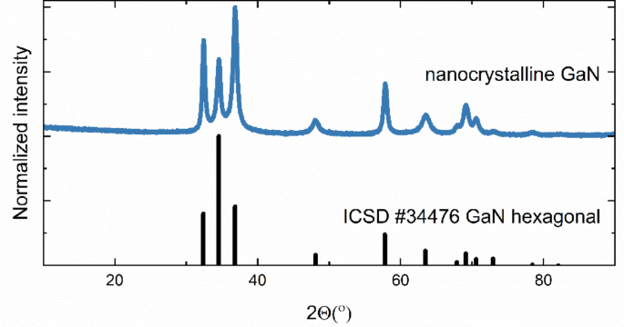
The obtained GaN nanocrystals have a hexagonal wurtzite structure, which was confirmed by XRD measurement, shown in (Fig. 1).
X-ray diffraction pattern of GaN nanocrystals.
According to the pattern (ICSD #34476), the obtained GaN nanocrystals have a pure structure with the broad reflections indicating nanosize. The average grain size was calculated by Rietveld analysis to be 12 nm. The absorption spectrum of GaN nanocrystalline powder is shown in (Fig. 2). By using the Kubelka-Munk function27 the energy band gap was determined to be 3.17 eV. Due to the nano-size of the particles, there are various defects in the structure, such as Ga and N vacancies, surface defects, or grain boundary defects. Therefore, the absorption edge shifts towards lower energies28 so the experimental value of the energy gap is smaller than the theoretical one of 3.4 eV29.
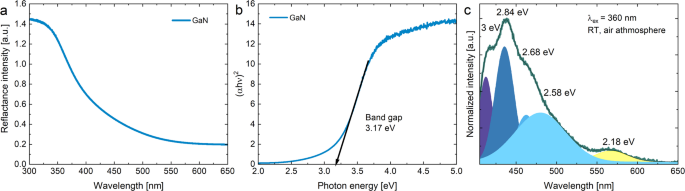
The reflectance absorption spectrum of GaN nanopowder (a), the experimental band gap (b) and the emission spectrum in the visible range upon λexc = 360 nm (c).
The wide band emission of GaN nanopowder in a range 405–650 nm with the maximum at 439 nm is shown in (Fig. 2c). Their deconvolution was performed to better understand the nature of the emission bands, resulting in five components with local maxima at 2.18 eV, 2.58 eV, 2.68 eV, 2.84 eV and 3 eV. The more intense bands 2.84 eV and 2.68 eV are most likely associated with VGa vacancies, and the remaining bands with VN vacancies28. The peaks at 3 eV, 2.84 eV are closest to the energy gap value, and may also be related to excitonic recombination30. The broad peak at 2.58 eV and the residual peak at 2.68 eV possibly relate to the presence of luminescent centers causing edge shifts for gallium and nitrogen vacancies31. The obtained material is also characterized by an undesirable yellow component of luminescence, which is caused by structural defects, indicating the imperfect structure of the obtained material2,32.
The research focuses on broadband white light emission (LIWE) characteristics and the accompanying photocurrent phenomenon. First, the studies show that a curve like a hysteresis loop can be observed by measuring the laser power density in the direction forward and backward. So far, two articles have been published attempting to explain the occurrence of hysteresis. These articles focus on carbon materials, diamond24and graphene33.
Due to its wide band gap, high thermal conductivity, and chemical stability, GaN is a suitable material for LIWE and photoconductivity investigation. The laser induced white emission spectra measured for GaN nanoceramics for both, visible and near-infrared regions are shown in Fig. 3a, b, respectively. It was characterized by broad bands whose intensity increases exponentially with excitation laser power density and leads to a blueshift of the bands. An increase in LIWE emission intensity starts after crossing the characteristic excitation threshold. The band extends from 400 to 2500 nm with a maximum of 1695 nm. For both regions, the emission threshold is estimated to be slightly above 1 kW/cm2. The emission intensity measurements were obtained using two detectors, which is why the emission intensity can be different, and the gap between the visible and near infrared regions results from the use of optical filters and the cutting of the excitation laser beam. Nevertheless, based on these spectra and the N parameter, which in both cases takes similar values, it can be suggested that this is a single broad band. It has also been reported that the two bands measured separately are actually one band34. Furthermore, experiments were performed for both regions, initiating hysteresis shape curve by measuring forward with increasing laser power density and then backward with decreasing laser power density. The results are shown in (Fig. 3c,d). In both cases, the characteristic properties of this phenomenon are preserved. The resulting loops are characterized by a threshold value followed by increased emission intensity. Moreover, saturation was demonstrated at high laser power densities. Furthermore, in the case of backward measurements, the N parameter for both ranges has higher values. Additionally, the emission threshold shifts towards higher power densities and saturation does not occur due to the lack of hysteresis. The SI (Figure S1) shows the CIE chromaticity diagram, demonstrating the objective color quality for both anti-Stokes and Stokes emissions. LIWE is characterized by a warm yellow color. Depending on the laser power density, the x and y coefficients locations differ, and as the laser power density increases, it is noticed that the emission color temperature changes towards white.
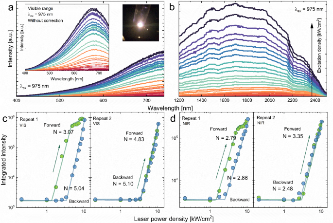
White emission intensity (a) near-infrared emission intensity (b) for GaN nanoceramics as a function of laser power density. The forward and backward cycles of LIWE in visible region (c) and near-infrared region (d). Inset the spectrum of LIWE without correction and the image of LIWE of light.
It was found that the investigated process is assisted by photoconductivity. Therefore, changes in sample resistance were measured depending on the laser power in cycles where the laser was turned on and off every 30 s. The changes were recorded at various voltage biases, as shown in (Fig. 4a). No changes in material resistance were observed at low laser powers, while at higher powers, a decrease in resistance was already observed. This is related to the threshold nature of both white emission and photocurrent. The dependence of resistance on the laser power density was plotted, and the excitation threshold was observed (Fig. 4b). Moreover, the applied voltage affects the initial resistance value. For 5 V, the resistance was the lowest, whereas the highest resistance was observed at 150 V. It should be noted that the resistance was dependent on the applied voltage up to 50 V, and then the saturation was observed. The initial value of resistance is similar for 50 V, 150 V, and 250 V. It can be observed that the photocurrent increases by two orders of magnitude with increasing excitation laser power. The excitation threshold was determined to be about 3 kW/cm2 (see Table S1 in SI).
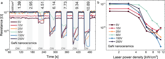
Photoresistance response measured in 30s cycles on/off at different voltage biases (a) and resistance dependence (b) for GaN nanoceramics.
White emission and photoconductivity were simultaneously performed in laser power density cycles (Fig. 5). The experiments were performed twice in closed (forward and backward) cycles. The differences can be noticed depending on whether the initial laser power density was low or high. For the first one, the hysteresis loop was observed for both LIWE and LIPC processes. However, hysteresis did not occur during measurements from a high initial laser power density.
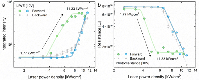
The laser power dependence of integrated intensity of LIWE (a) and the maximum of photoresistance of LIPC (b) measured in two consecutive measurement cycles: forward and backward (b) for GaN nanoceramics.
The LIWE mechanism has been explained many times, including as blackbody radiation35,36 thermal avalanche14,19,37 or intervalence charge transfer38,39,40,41. The characteristics of LIWE are mostly the same, so the mechanism should also be very similar. In this work, to explain the processes taking place, a proposed scheme (Fig. 6.) was used, in which the phenomenon is divided into stages: process before reaching the threshold value, multiphoton ionization and radiative recombination during irradiation after reaching the threshold value and possible occurrence of saturation with a high density NIR laser power.
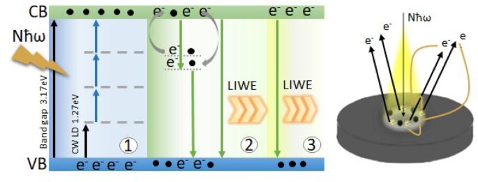
Scheme of proposed mechanism responsible for LIWE divided into 3 stages: (1) Process before threshold value, (2) Process after threshold value including multiphoton ionization and radiative recombination, (3) Saturation process.
At low laser power densities, no light is observed until the threshold is exceeded. This is due to the number of photons delivered to the sample surface. GaN nanoceramics is excited with an NIR laser with an energy of 1.27 eV, while the experimental value of the energy gap is 3.17 eV. With the laser power density increase, the probability of photons hitting the same electron increases, ejecting it of the valence band. Then, the multiphoton avalanche process leads to multiphoton ionization on the surface of the tested material. The phenomenon is nonlinear and with the increase of the laser power density, the intensity of emission increases. The dependence of LIWE intensity I(P) on the excitation laser power is usually characterized by the power law formula:
$$Ileft(Pright)propto:{P}^{::N}$$
(1)
where I(P) is the emission intensity, P is the excitation laser power, and N is related to the number of photons. This equation is used to describe multiphoton absorption transitions. Based on research in our group, where the dependence of power was plotted in different excited spot size it was found that the parameter N cannot be unambiguously treated as the number of absorbed photons. Based on this analysis, one should be more careful in connecting the nonlinearity of the process defined by the parameter N with the actual number of photons participating in the reaction31,42. The process of multiphoton ionization (MPI) in irradiated spot at the surface of GaN nanoceramics leads to the broadband white emission (LIWE) assisted by an ejection of hot electrons e− and may be described as:
$$GaN + MAleft( {Nhbar omega } right) to GaN^{ + } + ~e^{ – } ~ + {text{ }}LIWE + NR$$
(2)
where MA(Nħω) expresses the multiphoton absorption responsible for the multiphoton ionization of the GaN, GaN + is ionized GaN (cathode), LIWE represents laser induced white emission, and NR characterizes the nonradiative quenching and phonon emission processes contributing to the enhancement of thermally active processes. At higher laser power densities, more photons are transmitted to the sample surface, causing electrons to be emitted from the valence band to the conduction band. In addition, a radiative recombination process occurs. An electron from the conduction band recombines with a hole from the valence band, emitting a photon. This process is repeated until all possible emission centres are used. Saturation often occurs. The LIWE still occurs, but its intensity often remains unchanged or decreases. This is probably related to the confinement of some electrons, thus maintaining LIWE. The lack of new emission centres causes a lack of increase in emission intensity.
As explained above, during near-infrared laser irradiation of a sample in a dynamic vacuum, many processes occur, often overlapping. The hysteresis loop is probably formed not only due to photophysical processes but also because of morphological changes. Due to the fact that the measurements were performed depending on the density of the excitation laser beam on nanometric material, changes in the morphology of the sample may have occurred. When the measurement was performed from the lowest laser power, there could have been gradual ionization in GaN, an increase in temperature in the irradiated spot, and changes in morphology after obtaining a high power density. The following changes resulted in a different course when the laser power density decreased. This suggests an irreversible response of the material to the excitation condition. In turn, in the opposite case, the material was first irradiated with high laser power density, probably causing simultaneous ionization and another photophysical process explained in the proposed mechanism, changes in morphology, and high temperature at the beginning. Changing the density to a lower and then to a higher density does not cause changes in the emission intensity, which can confirm the conclusions drawn. Stręk et al.24 reported the hysteresis loop behavior for LIWE on diamond material. They explain this as an irreversible process caused by multiphoton ionization. The degree of ionization is related to the irradiation of the sample and the number of ionized atoms. This phenomenon can be used as an effective optical memory. In our case, the confirmation of irreversible process can be repeated measurement of the loop under the same conditions and at the same point, and likewise, the backward cycle, because under high density, the hysteresis loop does not occur. Additionally, based on an article from Zheng et al.23, where an experiment was performed in which two curves were recorded, one for the excitation laser turned on and the other for the excitation laser turned off, a change in the emission intensity was observed, which suggested that the process is not only thermal.
The broadband white light emission phenomenon began to be associated with the photocurrent that appears during sample irradiation. To characterize LIPC, the same formula as in the case of LIWE can be used because both phenomena are nonlinear and exhibit a threshold character. The dependence of photoresistance R on laser power density can be expressed by:
$$R~left( P right)~ propto P~^{{Npc}}$$
(3)
where Npc is related to the order of multiphoton ionization. The observed drop in resistance after reaching the threshold value is related to photoionization. After the material absorbs infrared photons, charge carriers are created. The higher laser density, the higher number of photons leading to stronger electron-hole recombination and, consequently, higher conductivity.
When discussing the LIWE and photocurrent phenomena, other factors are also considered, with one of the most important being the influence of temperature on the phenomena under study. LIWE was tested in many different luminescent materials, and it can be concluded that the shape of the emission does not depend on the host lattice. However, this phenomenon can be linked to the thermally assisted ionization process and strong optical nonlinearity. The differences resulting from the investigation are mainly associated with a change in the N parameter, depending on the material being tested. Interpretations of this behaviour should be considered. Since the experiments were performed on ceramics, the grains are as close to each other as possible, which reduces the energy localization in the laser spot and increases energy losses due to, for example, heat conduction and changes in the non-linearity of the process23. The temperature of emission at different power densities was calculated using the Planck equation (see Table S2 in Supporting Information)
$$:{B}_{lambda:}left(lambda:,Tright)=:frac{{2hc}^{2}}{{lambda:}^{5}}frac{1}{{e}^{hc/left(lambda:{k}_{B}Tright)}-1}$$
(4)
where h is Planck’s constant, c is the velocity of light, λ is the wavelength (nm), and kB is Boltzmann’s constant. The spectrum is dependent on the temperature of the sample. Based on this calculation the temperature was fitting with a good comparison both in relation to the theoretic temperature values associated with blackbody radiation and in relation to the fit of these values in the CIE chromaticity diagram. Despite the good fit of the temperature to Planck’s law, LIWE is mainly caused by the sample ionization process. As shown in articles on other materials, significant differences are observed between the temperature values during LIWE. Using measurements with a thermal camera, the maximum temperature is read at about 1230 K23. In the case of other articles, measurements of luminescence nanothermometry, where the emission intensity ratio 2H11/2 ◊ 4I15/2 to 4S3/2 ◊ 4I15/2 of Er3+ ion is used as a temperature probe, the observed maximum temperature takes values of about 900 K39. Then, it can be assumed that such differences can be observed in these studies as well, at least because the temperature values based on black body radiation are directly related to a very small point on the sample surface during emission, while the thermal camera shows values where the spot is wider. In connection with this, the temperature distribution is not clearly defined, and the small size of the spot in the laser focus does not allow for direct, accurate measurement without luminescence thermometry. Here one should be careful because, as described above, this method gives values much lower than the blackbody fitting. The question still remains how to properly determine the temperature, such studies are required in the future.