Lineker had originally been due to front coverage of the tournament for the BBC, but he announced in May he’d be leaving the corporation earlier than planned following an antisemitism row.
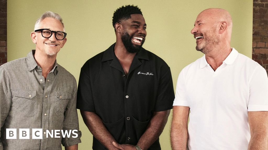
The visualised podcast, which is hosted by Lineker, Alan…
Lineker had originally been due to front coverage of the tournament for the BBC, but he announced in May he’d be leaving the corporation earlier than planned following an antisemitism row.
The visualised podcast, which is hosted by Lineker, Alan…