
Figure 1 illustrates the circuit of the proposed structure, which consists of a single DC source, 10 unidirectional power electronic switches, 3 capacitors, and a diode. Switches S3 and S5 lack anti-parallel diodes, and their simultaneous activation enables the simultaneous charging of capacitors C2 and C3. Additionally, capacitor C1 is charged through the activation of switch S8. Using this simple algorithm, an 11-level output voltage is achieved. The switched capacitors stabilize at the desired voltage levels without the need for auxiliary circuits or sensors. The voltage level of capacitor C1 equals the input source voltage, while the voltage levels of capacitors C2 and C3 are half the input voltage. In Fig. 1, the maximum blocking voltage (MBV) of the switches and diode is indicated. Despite the output voltage boost factor being 2.5 times the input voltage, the maximum voltage stress on all components is lower than this value, which is a significant advantage of the proposed structure. The switching method for the proposed structure is presented in Table 1. In this table, the value “1” indicates that the corresponding switch is ON during the generation of the specified voltage level, while “0” indicates that it is OFF. Besides, “C” means charging, “D” means discharging, and “-” means no change in capacitor voltage.
Proposed inverter structure.
Operating States
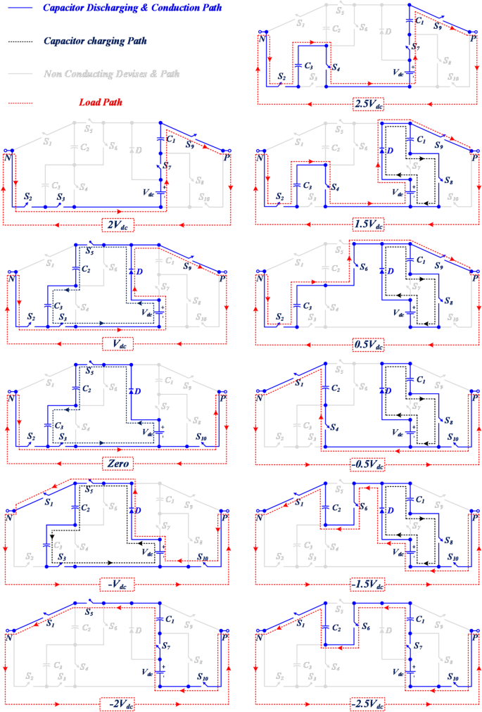
Figure 2 illustrates the operating states and current paths during the positive and negative half-cycles. For each voltage level, only 4 of the 10 switches in the structure are turned ON, which is a significant advantage as it reduces conduction losses. The switching states for the positive half-cycle are described as follows:
State A: When switches S2, S4, S7, and S9 are ON, capacitors C1 and C3 discharge, generating the voltage level 2.5Vdc.
State B: Current flows through switches S2, S3, S7, and S9, and with the discharge of capacitor C1, the sum of the input source voltage and capacitor C1 generates the output voltage.
State C: In this state, switches S2, S4, S8, and S9 are turned ON, capacitor C1 charges, and capacitor C3 discharges to generate the voltage level 1.5Vdc.
State D: Switches S2, S3, S5, and S9 are turned ON, and capacitors C2 and C3 are simultaneously charged to 0.5Vdc. In this state, the voltage level Vdc is generated by the DC source.
State E: Current flows through switches S2, S6, and S9, generating the voltage level 0.5Vdc with the discharge of capacitor C3. In this state, capacitor C1 charges through switch S8, which is connected in parallel with the DC source.
State O: To generate the zero voltage level, switches S2, S3, and S10 are turned ON. In this state, capacitors C2 and C3 are simultaneously charged through switch S5.
Current paths for load current and capacitor charging current in the proposed structure.
Switching method
Various methods have been introduced for controlling and generating pulse signals for switches in multi-level switched capacitor inverters. PWM, NLM, SVM, and SHE are among the most important switching methods, and they have been widely used over the years, each with its own advantages and disadvantages20,21,22,23. The SHE and NLM techniques fall under the category of low-frequency switching methods, while the SVM and PWM techniques are classified as high-frequency switching methods. Each of these methods can be implemented in the proposed structure. The proposed structure uses sinusoidal PWM modulation to shift the switching level, and the components of this modulation are shown in Figure 3. As illustrated in Figure 3-a, to generate an 11-level output voltage, 10 carrier signals (Vcar) with identical amplitude and switching frequency are needed, along with one reference signal (Vref). By comparing the reference signal with the carrier signals, the switching pulses corresponding to each voltage level are generated. The modulation index can be defined by the following relation:
$${m_a}=frac{{{{hat {V}}_{ref}}}}{{5{{hat {V}}_{car}}}}$$
(1)
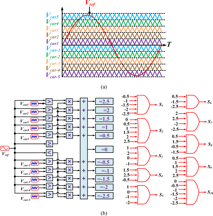
Modulation technique (LS-PWM), a PWM signal generation scheme, b) Logical circuit for pulse generation.
Capacitor design
One of the key parameters in designing a multi-level switched capacitor inverter is selecting the appropriate capacitor size for the structure being used. If the capacitor size is less than the correct and suitable value, the voltage ripple across the capacitor will increase. This not only reduces the quality of the output voltage but also increases the capacitor charging current and the associated ripple losses. Additionally, if the capacitor size is greater than the correct and appropriate value, the cost and size of the inverter will increase. Therefore, in order to improve the inverter’s efficiency, the design and calculation of the appropriate capacitor size is of high importance. To select the capacitor size, the maximum voltage ripple across the capacitor during the switching process is calculated. For this purpose, the range in which each capacitor experiences the maximum discharge duration (MDD) is considered. To identify these time intervals, Figure 4, which illustrates the charging and discharging process of capacitors at different output voltage levels, can be used.
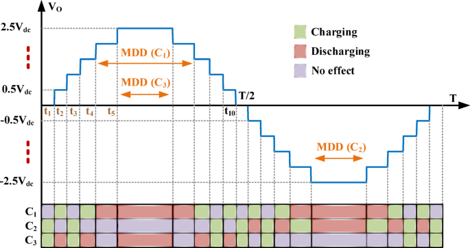
Charging and discharging of capacitors based on output voltage levels.
Based on Figure 4, the maximum discharge duration (MDD) for capacitor C1 occurs during one quarter of the period from time t4 to T/2-t4. Similarly, the maximum discharge duration (MDD) for capacitors C2 and C3 occurs during one quarter of the period from time t5 to T/2-t5. Based on the symmetry in the output voltage waveform, the discharge time intervals for the capacitors are described for one-quarter of the period. To calculate the discharge energy and account for the full discharge duration, a factor of two is used. The moments indicated in Figure 4 are determined using Eq. (2), where Nl represents the number of output voltage levels. Using this equation, the moments t1 through t5 can be written as Eq. (3)24:
$${t_x}=frac{{arcsin left( {frac{{2x – 1}}{{{N_l} – 1}}} right)}}{{2pi f}}$$
(2)
$$begin{gathered} {t_1}=frac{{arcsin left( {{1 mathord{left/ {vphantom {1 {10}}} right. kern-0pt} {10}}} right)}}{{2pi f}},,,,,,{t_2}=frac{{arcsin left( {{3 mathord{left/ {vphantom {3 {10}}} right. kern-0pt} {10}}} right)}}{{2pi f}},,,,,,,{t_3}=frac{{arcsin left( {{5 mathord{left/ {vphantom {5 {10}}} right. kern-0pt} {10}}} right)}}{{2pi f}},,, hfill \ begin{array}{*{20}{c}} {}&{} end{array},,,,{t_4}=frac{{arcsin left( {{7 mathord{left/ {vphantom {7 {10}}} right. kern-0pt} {10}}} right)}}{{2pi f}},,,,,,,{t_5}=frac{{arcsin left( {{9 mathord{left/ {vphantom {9 {10}}} right. kern-0pt} {10}}} right)}}{{2pi f}} hfill \ end{gathered}$$
(3)
Since the capacitors are placed in the load path to generate output voltage levels and discharge, the current passing through the capacitors can be considered as the load current (Io). Therefore, the amount of charge discharged from the capacitors during specific time intervals can be expressed by the following equations:
$$Delta {Q_{{C_1}}}=2int_{{{t_4}}}^{{T/2 – {t_4}}} {{I_o}} sin left( {omega t – varphi } right)dt$$
(4)
$$Delta {Q_{{C_2}}}=Delta {Q_{C3}}=2int_{{{t_5}}}^{{T/2 – {t_5}}} {{I_o}} sin left( {omega t – varphi } right)dt$$
(5)
If the voltage ripple percentage of the capacitors (ΔVripple) is within the standard range and less than 10%, the minimum required capacitance can be expressed using relations (6) and (7):
$${C_1} geqslant frac{{2{I_o}}}{{2pi f times {V_{dc}} times {V_{ripple}}}}left( {cos left( {0.7754 – varphi } right) – sin varphi } right)$$
(6)
$${C_2},{C_3} geqslant frac{{2{I_o}}}{{2pi f times left( {0.5{V_{dc}}} right) times {V_{ripple}}}}left( {cos left( {1.12 – varphi } right) – sin varphi } right)$$
(7)
The selected capacitor capacitance must be higher than the calculated capacitance, and thus, the first standard capacitor with a value greater than the calculated capacitance (according to the capacitor’s datasheet) is chosen.
Capacitor charging current
One of the main challenges in the design and use of multilevel switched capacitor inverters is the capacitor charging current. This current is generated during the charging of the capacitors through the input voltage source, and at the moment of inverter startup, it is very high. If the capacitor charging current is not controlled, it can lead to damage to the circuit components, reduced capacitor lifespan, and decreased converter efficiency. Various methods have been proposed for controlling the capacitor charging current, among which the most important are the use of current-limiting resistors25 and the use of current-limiting inductors26, which play a significant role in reducing and controlling the capacitor charging current. In this paper, as shown in Figure 5, an inductor (Lr) in parallel with a reverse-parallel diode (Dr) is used to limit the capacitor charging current. The current-limiting inductor is connected in series with the input voltage source, preventing the capacitor from drawing a large instantaneous charging current. The size of the inductor must be properly chosen, as if the inductor is larger than the required value, it may cause disturbance in the dynamic response of the inverter. For proper operation, the condition of Eq. (8) must be satisfied, and the switching frequency (fsw) must be greater than the resonance frequency (fr) resulting from the current-limiting inductor and capacitor. The size of the current-limiting inductor can be calculated using Eq. (9):
$${f_{sw}}>frac{1}{{2pi sqrt {{L_r}C} }}={f_r}$$
(8)
$${L_r} geqslant frac{1}{{{{left( {2pi {f_{sw}}} right)}^2}C}}$$
(9)
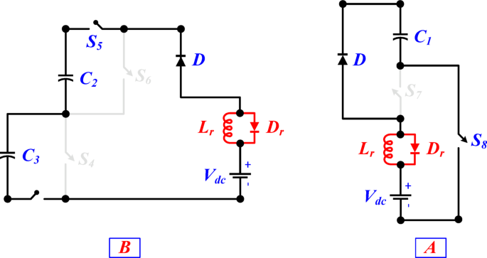
Equivalent circuit of soft charging of capacitors with a current-limiting inductor, (a) Soft charging of capacitor C1, (b) Soft charging of capacitors C2 and C3.