by Bob Francis, Fort Worth Report
December 14, 2025
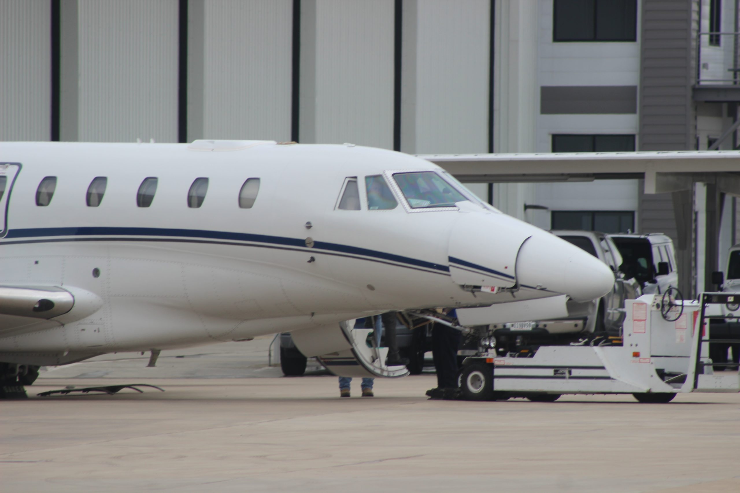
Companies and individuals with private jets will have a new spot to hang out at Fort Worth Meacham International Airport.
Private aviation real estate developer and operator Sky Harbour has signed a lease with the city of Fort Worth to operate a boutique dedicated airplane service location at the 100-year-old airport.
The West Harrison, New York-based company said it plans to break ground in late 2026 on a $17 million complex consisting of a pair of 32,000-square-foot hangars capable of housing the latest ultra long-range business jets. The Meacham location is expected to create hundreds of local jobs, according to the company.
Unlike traditional fixed base operators, Sky Harbour offers home base operations, which means they are closed to transient traffic, providing tenants with security and more customized services. Sky Harbour locations offer pilot lounges, private offices, briefing rooms and hospitality areas
Sky Harbour is rapidly expanding its footprint across the U.S., building out high-end, boutique private hangar space for aircraft owners at key airports across the country.
According to the city of Fort Worth, the annual revenue generated from the ground lease at Meacham is about $95,725.
Sky Harbour has also leased space at Dallas Love Field Airport and Dallas Executive Airport.
The company currently has deals or is operating at 23 airports in the U.S., with nine locations in operation and 14 under development.
Funding for Westside Village infrastructure
On Dec. 8, the taxing district covering the Near West Side approved $45 million in infrastructure funds for the $1.7-billion Westside Village development.
The project, from FW Westside RE Investors, a partnership between Larkspur Capital and Keystone Group, will transform the 37 acres that once housed Fort Worth ISD’s former headquarters at 100 N. University Drive and other nearby sites, including the current Autobahn Fort Worth location. At full build-out, Westside Village will consist of 880,000 square feet of office space, 238,000 square feet of retail, a boutique hotel and 1,785 residential units.
Fans of Fort Worth
Lasko, a fan and heater manufacturer, has renewed and expanded its lease at 900 Terminal Road in Fort Worth. Lasko had been occupying 218,076 square feet of space at the location but has now expanded its footprint to 468,726 square feet. Transwestern Real Estate Services brokered the renewal and expansion.
Coffee, meet pie
White Rhino Coffee, a Dallas-based specialty coffee company known for its community-driven cafes and craft-focused approach, has purchased Emporium Pies, a North Texas dessert destination, with a location at 411 S. Main St. in Fort Worth. White Rhino has a location in Arlington.
Bagging it
Bag Supply Co. has leased an 18,000-square-foot industrial building in Point 820 in East Fort Worth to expand and relocate its only distribution center outside its home state of Alabama.
The company is taking up residence at 5911 E. Rosedale St., where it gained roughly 8,000 square feet of extra operating space and has access to Loop 820. Bag Supply has relocated from nearby Everman in tandem with a lease expiration.
“Bag Supply chose this project for the immediate freeway access and make-ready space, which was well-suited for its needs,” said Cade Navarro, broker associate in the Fort Worth office of Dallas-based Bradford Commercial Real Estate Services. Navarro represented the tenant, a division of Field Packaging Solutions in Moody, Alabama.
The industrial structure was fully renovated in summer 2024 as part of a major upgrade at Point 820, a 31-building project totaling 587,725 square feet. Brett Carlton and Forrest Cook of Stream Realty Partners represented the Boston-based landlord, LRF3 Dal Rosedale.
Do you have something for the Bob on Business column? Email Bob Francis, business editor for the Fort Worth Report, at bob.francis@fortworthreport.org.At the Fort Worth Report, news decisions are made independently of our board members and financial supporters. Read more about our editorial independence policy here.
This <a target=”_blank” href=”https://fortworthreport.org/2025/12/14/bob-on-business-fort-worth-lands-dedicated-corporate-jet-services-company/”>article</a> first appeared on <a target=”_blank” href=”https://fortworthreport.org”>Fort Worth Report</a> and is republished here under a <a target=”_blank” href=”https://creativecommons.org/licenses/by-nd/4.0/”>Creative Commons Attribution-NoDerivatives 4.0 International License</a>.<img src=”https://i0.wp.com/fortworthreport.org/wp-content/uploads/2021/04/cropped-favicon.png?resize=150%2C150&quality=80&ssl=1″ style=”width:1em;height:1em;margin-left:10px;”>
<img id=”republication-tracker-tool-source” src=”https://fortworthreport.org/?republication-pixel=true&post=326326&ga4=2820184429″ style=”width:1px;height:1px;”><script> PARSELY = { autotrack: false, onload: function() { PARSELY.beacon.trackPageView({ url: “https://fortworthreport.org/2025/12/14/bob-on-business-fort-worth-lands-dedicated-corporate-jet-services-company/”, urlref: window.location.href }); } } </script> <script id=”parsely-cfg” src=”//cdn.parsely.com/keys/fortworthreport.org/p.js”></script>