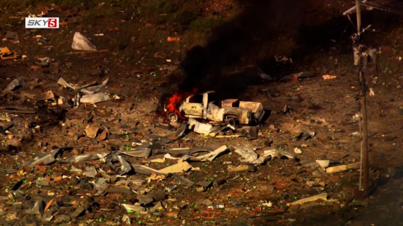
In a bid to advance large-format imaging, Canon has just patented a new semiconductor wiring structure that could improve the performance, reliability, and production yield of high-resolution sensors. It’s more than smaller and smarter wires. Think of it like a more efficient and robust design for large image sensors. Check out the highlights below.
Modern image sensors, especially full-frame and larger formats used in cinema and photography, require extremely fine electrical wiring to connect pixels across the chip. But as sensors get physically bigger (sometimes over 36mm wide) conventional lithography equipment hits a hard limit: it simply can’t expose the entire sensor area in one shot. That’s where Canon’s innovation steps in. Canon’s new patent outlines a way to strategically widen wiring segments in overlap regions: those areas where two photomask exposures meet on a large wafer. By increasing the width of these “bridging” sections while keeping the rest of the wiring narrow (less than 180 nanometers), Canon can dramatically reduce risks of:
-
Misalignment between exposure zones
-
Broken or short-circuited signal lines
-
Noise and image artifacts, especially near pixel rows
This architecture uses damascene wiring which is a process where trenches are carved into an insulating layer, filled with copper, and polished flat. It’s the gold standard for modern CMOS imaging sensors.


In practice, this innovation enables Canon to:
-
Build larger and more reliable CMOS sensors without compromising pixel density
-
Deliver cleaner signals from edge to edge, especially important in 8K+ resolution sensors
-
Improve manufacturing yields, which helps lower costs in production
The patent also integrates a clever pixel layout trick: thickened wiring segments are mirrored even in pixels that don’t lie in exposure overlap regions. This helps maintain uniform image quality and avoids visible artifacts in the final image. Whether Canon will apply this to upcoming Cinema EOS, RF mirrorless, or even industrial sensors, is not stated. But from a tech perspective, it’s a smart move toward future-proofing high-resolution imaging.


What makes this patent stand out is not flashy resolution numbers or marketing jargon, but rather the underlying infrastructure that enables Canon to scale up its sensors safely and efficiently. As demands rise for larger sensors, whether in cinema, surveillance, or computational imaging, this kind of semiconductor engineering is what keeps innovation possible. Hence, Canon’s latest patent is a great example of subtle but essential sensor design thinking. By tweaking how wires are routed across large chips, Canon is laying the groundwork for more powerful and reliable large sensor cameras in the years ahead.
Canon Store and Products

