Araqchi says no formal negotiations have taken place, only messages exchanged through intermediaries
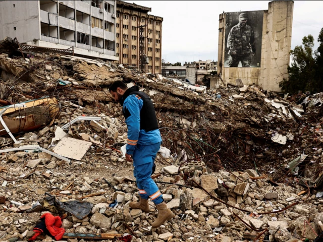
A paramedic walks among the rubble at a site damaged in an Israeli strike, amid escalating hostilities between Israel and Hezbollah, as the…
Araqchi says no formal negotiations have taken place, only messages exchanged through intermediaries
A paramedic walks among the rubble at a site damaged in an Israeli strike, amid escalating hostilities between Israel and Hezbollah, as the…
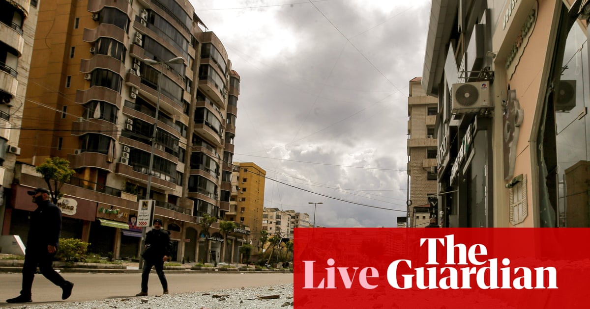
China’s foreign minister has said that a “glimmer of hope” for peace has emerged due to moves to stop the war in the Middle East, despite Tehran vowing to keep fighting.
Wang Yi urged dialogue in…

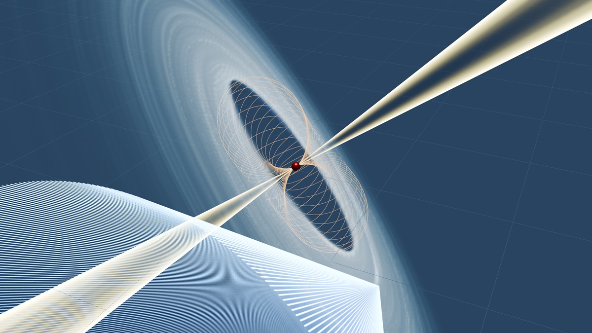
When you reach into a bucket of ice, open your front door on a snowy day, or feel the tingle of menthol toothpaste, a protein in your nerve cells called TRPM8 springs into action, opening like a tiny gate to send a “cold” signal to…


Cinegy will show how its solutions answer the real challenges facing content creators and broadcasters today at NAB Show 2026 (Booth N809, Las Vegas Convention Centre, 19-22 April). The presentations will show how highly refined software…