Qaasid News
Download Our App
Latest News from Pakistan
Women’s Basketball Wraps Non-Conference Play With Loss At Notre Dame
December 22, 2025
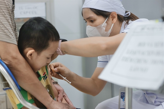
Hanoi says infectious diseases under control despite rise in measles and hand, foot and mouth cases
December 22, 2025
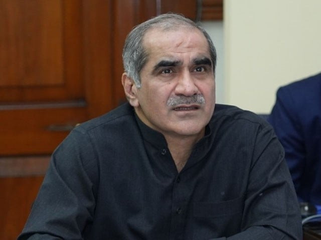
Three in race as PIA bid opens tomorrow – Dawn
December 22, 2025
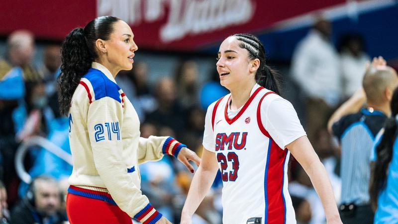
SMU’s Defense Leads Mustangs To A 74-62 Win Over Southern
December 22, 2025
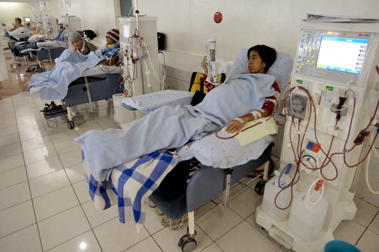
More young Filipinos getting chronic kidney disease — and they learn too late
December 22, 2025
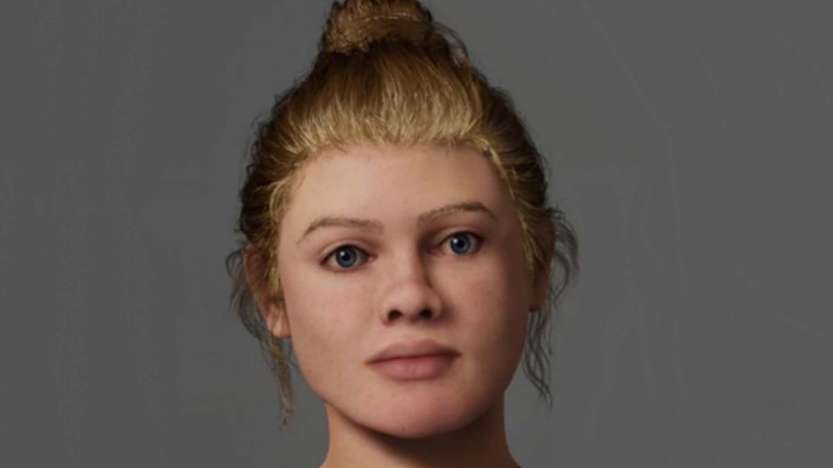
Ancient DNA Reveals Surprising Truth of Beachy Head Woman’s Identity : ScienceAlert
December 22, 2025
At key conference, opposition demands credible elections, smooth transfer of power
December 22, 2025
Famous Idaho Potato Bowl Pregame Press Conference Transcript
December 22, 2025
Five Gophers Score Double Digits in Win Over Campbell
December 22, 2025
PML-N leaders back new democracy charter
December 22, 2025